Télécharger le fichier original (Mémoire de fin d’études)
Doping of (Si)GeSn
A big step towards the co-integration of group IV photonics with CMOS circuits was recently made by research teams in the US, with electrically pumped lasing in GeSn up to 100 K. [32], [33] In CEA-LETI, we have so far used in-situ doped Ge in our pin Light Emitting Devices (LEDs) and Photo-Detectors (PDs). [50] Such Ge:P or Ge:B layers were grown at somewhat elevated temperatures (350°C) compared to the optically active, high Sn content GeSn layers (313°C). Growth at such an elevated temperature might have resulted in Sn segregation and precipitation, deteriorating the performance of the pin structures in our previous investigations. [51] To reproduce electrically pumped lasing [32], [33] and, beyond that, achieve electrically pumped lasing at high temperatures, it is necessary to investigate the low temperature doping of GeSn. Ion implantation together with mainstream anneals are not really suitable for doping GeSn. The high thermal budget of typical post-implantation annealing that is mandatory to heal defects and incorporate dopants into electrically active lattice sites would indeed result in Sn surface segregation and precipitation. [52] Another possibility is to in-situ dope GeSn during the epitaxial growth itself. This way, dopants are incorporated into the lattice as the layer grows, without any annealing requirement, afterwards. Sn segregation and precipitation are thus avoided, as shown in the literature for GeSn:B [46] and GeSn:P [53].
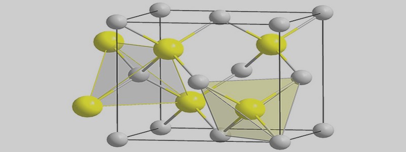
Doping relies on the incorporation of foreign elements into substitutional lattice sites. These foreign elements have one electron more (n-type) or less (p-type) than the matrix element, shown in Figure I.7, resulting in the supply of free electrons (n-type) or holes (p-type) for electrical conduction.
The in-situ doping of GeSn has not thoroughly been investigated. Vincent et al. [46] studied the in-situ boron doping of GeSn with Sn contents of around 7%. They found that the introduction of B2H6 in the gas mixture and, therefore, the incorporation of boron (B) into the GeSn lattice, resulted in a reduction of the Sn content, which was explained by a competition between Sn and B for incorporation into the lattice. Rutherford backscattering (RBS) and micro-Hall measurements were used to unambiguously determine the Sn and B contents in the studied layers. Margetis et al. [54] investigated this phenomenon in more details. They found from RBS and Secondary Ion Mass Spectrometry (SIMS) measurements that Sn content reductions were due to a GeSn:B growth rate increase, reducing the amount of time Sn atoms had to incorporate and, hence, the amount of Sn.
Epitaxial Growth and Nanosecond Laser Annealing of GeSn/SiGeSn Heterostructures In-situ phosphorus doping of GeSn was studied even less. Margetis et al. [53] reported increased Sn contents for GeSn:P compared to intrinsic GeSn. It was attributed to the presence of P atoms on the surface, catalyzing the reduction of SnClx* (where * denotes an open surface site) with the formation of PClx (g). Margetis et al. did not evidence any dependence of the Sn content or GeSn growth rate on the PH3 flow supplied, however.
Fang et al. were, to our knowledge, the first to study SiGeSn in-situ doping in Chemical Vapor Deposition (CVD). [56] Ge2H6, B2H6 and SnD4, the Sn precursor used before SnCl4, were then selected as precursors. More specific precursors like Si3H8, SiGeH6, and some designer hydrides, e.g. P(GeH3)3 and P(SiH3)3, were also evaluated. Growth temperatures between 320 °C and 345 °C were used and Sn contents ranging from 2% to 8% probed. Growth rates were two to three times higher when dopant precursors were added to the gaseous mixture. SiGeSn layers lattice matched to the Ge buffer underneath were grown. B doping levels between 5×1019 cm-3 and 2×1020 cm -3 were obtained, together with P doping levels around 1019 cm-3 (from Hall measurements and contactless Infra-Red spectroscopic ellipsometry). Wirths et al. explored the growth of in-situ doped SiGeSn with Ge2H6, Si2H6, and SnCl4 [57], i.e. the precursors used in the present studies. The growth temperature was 425 °C, then. B2H6 diluted at 100 ppm in H2 and undiluted PH3 were adopted as dopant sources. Wirths et al. used an AIXTRON TRICENT Reduced Pressure-CVD system with N2 as a carrier gas, a showerhead for vertical gas injection, and a thermocouple in close proximity with the wafer to monitor the temperature. Such a hardware is quite different from ours, with a horizontal laminar flow of H2 over the wafer surface supplying precursors to it and a dedicated pyrometer monitoring the wafer plate’s backside temperature. This seemed to result in growth temperature differences between setups around 75 °C. More precisely, a growth temperature of 425 °C in the AIXTRON tool is comparable to 350 °C in our Epi Centura tool. Wirths et al. found reduced layer resistivities at high B2H6 partial pressures and increased layer resistivity at high PH3 partial pressures due to the reduced layer quality because of the high, undiluted flow of PH3. The introduction of dopant precursors did not significantly change the growth rates in their case. They achieved electrically active carrier concentrations (determined by electrochemical capacitance voltage (ECV) measurements) of 2×1019 cm-3 (p-type) and 8×1019 cm-3 (n-type), with a good SiGeSn:B or SiGeSn:P crystalline quality. Epitaxial Growth and Nanosecond Laser Annealing of GeSn/SiGeSn Heterostructures
Strain Relaxation in (Si)GeSn
on (1 1 1) ⃑⃑⃑ ̅ ⃑⃑⃑⃑
( 1) and (1 1 1 ) ( 2) planes intersect. [58] (b) Scanning transmission electron microscopy (STEM) images of nominally constant composition, thick GeSn and superimposed the corresponding Energy Dispersive X-ray (EDX) profile. [59]
Thick, relaxed and high Sn content (Si)GeSn layers are required to fabricate performant devices. Al-Kabi et al. and Aubin et al. [51], [59], [60] found, when growing relaxed, constant composition GeSn, a lower Sn content GeSn layer with a high misfit dislocation density close to the Ge SRB. Above the critical thickness [61], the Sn content spontaneously increased when the compressive strain started to plastically relax. Dou et al. and Assali et al. [58], [61] reported a spontaneous Sn content enhancement resulting in Hagen-Strunk misfit dislocation multiplication. [62], [63] The generation of additional 60 ° dislocations with complementary
Burger’s vector ⃑ resulted in the interaction of 60 ° dislocations gliding along different { 1 1 1 } planes. When meeting each other, they intersected thanks to a cross-slipping mechanism and formed sessile Lomer dislocations, as shown in Figure I.9 (a). The formed Lomer dislocations were prohibited from gliding and the threading arms of the 60 ° mixed dislocations annihilated. This resulted in the formation of a self-assembled dislocation network, with almost defect free layers grown on top, as shown in Figure I.8 (b). In addition, strain relaxation resulted in higher Sn incorporation. [58], [59], [61], [64], outlining that strain was the main force driving the incorporation of Sn.
Table des matières
Introduction
Chapter I : Challenges of Growing and Doping GeSn
I.1 Epitaxy
I.1.1 The concept of Epitaxy
I.1.2 The concept of plastic strain relaxation
I.1.3 Critical thickness for plastic strain relaxation
I.1.4 Lattice defects
I.2 The (Si)GeSn material system
I.2.1 (Si)GeSn: a direct band-gap group IV semiconductor
I.2.2 Doping of (Si)GeSn
I.2.3 Strain Relaxation in (Si)GeSn
I.3 Thermal Treatement
I.3.1 Thermal stability of (Si)GeSn
I.3.2 Heat Transfer Mechanism
I.3.3 Atomic diffusion
I.3.4 Annealing Methods
I.4 Laser-Matter Interaction
I.4.1 Liquid phase recrystallization
I.4.2 Segregation
I.4.3 Dopant Activation
I.5 Conclusion
Chapter II : Experimental Techniques
II.1 Reduced Pressure Chemical Vapour Deposition (RP-CVD)
II.1.1 Chemical Vapour Deposition
II.1.2 The Epi Centura 5200 cluster tool
II.1.3 Growth Mechanisms
II.2 Nanosecond Laser Annealing (NLA)
II.2.1 The Nanosecond Laser Annealing tool
II.2.2 In-situ Time Resolved Reflectivity Measurements
II.3 X-Ray Diffraction
II.3.1 Introduction
II.3.2 Measurement Modes
II.4 Surface Characterization Techniques
II.4.1 Atomic Force Microscope (AFM)..
II.4.2 Scanning Electron Microscopy (SEM)
II.5 Transmission Electron Microscope (TEM)
II.6 Composition Characterization Techniques
II.6.1 Secondary Ion Mass Spectrometry (SIMS)
II.6.2 Wavelength Dispersive X-ray Fluorescence (WDXRF)
II.6.3 Energy Dispersive X-ray Spectroscopy (EDX)
II.6.4 X-ray Photoelectron Spectroscopy (XPS)
II.7 Electrical Characterization Techniques
II.7.1 Transmission Line Method (TLM)
II.7.2 Four Point Probe measurements (4PP)
II.7.3 Electrochemical Capacitance Voltage (ECV) profiling
II.8 Conclusion
Chapter III : In-Situ B and P Doping of GeSn
III.1 Intoduction
III.2 Confirmation of new growth parameters
III.3 Layer thickness and Sn content determination
III.4 Incorporation of Sn and dopants into the GeSn lattice
III.5 Catalytic impact of dopants on growth rate
III.6 Surface morphology and roughness
III.7 Conclusions
Chapter IV : In-Situ B and P Doping of SiGeSn
IV.1 Introduction
IV.2 Impact of dopant precursors on crystalline quality and layer thickness
IV.3 Impact of dopant precursors on composition
IV.4 Catalytic impact of dopants on growth rate
IV.5 Surface morphology and roughness
IV.6 Incorporation and activation of dopants in the SiGeSn lattice
IV.7 Conclusions..
Chapter V : Nanosecond Laser Annealing of In-Situ B Doped
V.1 Introduction
V.2 Impact of the substitutional B concentration on the melt threshold
V.3 Single pulse nanosecond laser annealing: Dopant activation
V.4 Single pulse nanosecond laser annealing: Surface morphology evolution
V.5 Single pulses nanosecond laser annealing on Ge:B: Crystalline structure
V.6 Multipulse nanosecond laser annealing: Surface morphology evolution
V.7 Multipulse nanosecond laser annealing: Crystalline structure evolution
V.8 Multipulse nanosecond laser annealing: Dopant activation
V.9 Conclusions..
Chapter VI : Single Pulse Nanosecond Laser Annealing of
VI.1 Introduction
VI.2 Wafer uniformity
VI.3 Impact of different Sn contents on Time Resolved Reflectivity Response
VI.4 Effect of Nanosecond Laser Annealing on Surface Morphology
VI.5 Effect of Nanosecond Laser Annealing on Crystalline Structure
VI.6 Effect of Nanosecond Laser Annealing on Sn redistribution
VI.7 Conclusions.
Chapter VII : Multi Pulse Nanosecond Laser Annealing of GeSn
VII.1 Introduction
VII.2 Multi Pulse NLA – Evolution of Time Resolved Reflectivity
VII.3 Multi Pulse NLA – Evolution of surface structure at the melt threshold
VII.4 Multi Pulse NLA – Evolution of surface morphology at the full melt threshold
VII.5 Multi Pulse NLA – Evolution of crystalline structure at the melt threshold
VII.6 Multi Pulse NLA – Sn redistribution
VII.7 Conclusions
Chapter VIII : Nanosecond Laser Annealing of Phosphorus Implanted
GeSn
VIII.1 Introduction..
VIII.2 Time Resolved Reflectivity evolution
VIII.3 P implanted GeSn NLA – Surface Morphology Evolution
VIII.4 P implanted GeSn NLA – Crystalline Structure
VIII.5 P implanted GeSn NLA – Tin and phosphorus redistribution
VIII.6 P implanted GeSn NLA – Solid Phase Epitaxial Regrowth
VIII.7 Conclusions
Conclusions and Perspectives
Appendix A : Résumé Français Etendu
Appendix B : NLA of Pseudomorphic GeSn Layers : Impact of Sn Content
Appendix C : Multi Pulse Nanosecond Laser Annealing of GeSn
Appendix D : GeSnOI Mid-Infrared Laser Technology
Appendix E : Room Temperature Optically Pumped GeSn Microdisk Lasers
Appendix F : Up to 300 K Lasing with GeSn-On-Insulator Microdisk Resonators
Appendix G : Valorization
Télécharger le rapport complet